
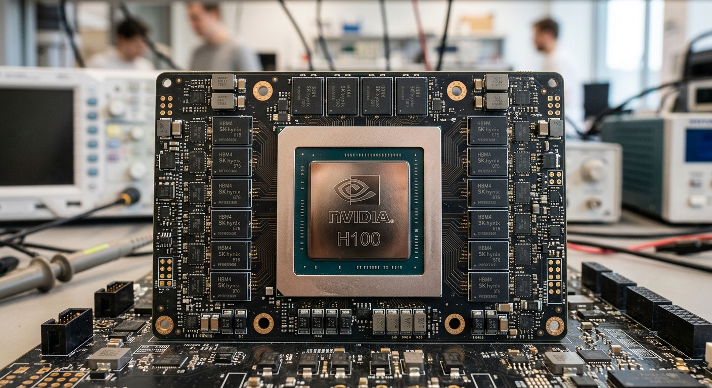
NVIDIA has officially taped out the Rubin R100 data center GPU, transitioning to TSMC’s N3P process node and introducing the industry’s first enterprise implementation of 8-Hi HBM4 memory stacks. The architecture drastically alters the memory-to-compute ratio for high-performance computing (HPC) clusters, delivering up to 16 TB/s of aggregate memory bandwidth while adhering to a strict 1200W thermal design power (TDP) limit.
- Shattered Memory Walls: The transition to a 2048-bit interface per HBM4 stack effectively doubles the memory bandwidth over the Blackwell B200, resolving localized interconnect saturation during multi-modal model training.
- Native FP4 Compute Pipelines: Hardware-level integration for 4-bit floating-point (FP4) operations allows hyperscalers to double inference density per rack without expanding their data center thermal footprint.
- Liquid Cooling Mandates: Reaching a 1200W TDP baseline per accelerator effectively obsoletes standard air-cooled server chassis, forcing enterprise environments to transition entirely to direct-to-chip (D2C) liquid cooling infrastructure.
Technical & Architectural Context
The Rubin R100 architecture abandons the traditional monolithic reticle limit approach, fully committing to a multi-die logic implementation on TSMC’s CoWoS-L advanced packaging. By separating the primary compute dies from the I/O and memory controllers, NVIDIA optimizes yield on the highly competitive N3P node. This structural shift allows the R100 to allocate dedicated silicon real estate exclusively to next-generation Tensor Cores engineered for extreme sparsity.
On the compute front, the R100 radically alters precision scaling. While TF32 operations remain critical for legacy algorithmic computations, the architectural emphasis heavily favors low-precision, high-throughput workloads. FP8 and FP4 processing pipelines now operate with shared exponent routing, drastically reducing SRAM fetch latencies during massive transformer layer matrix calculations.
For scientific computing workloads—particularly molecular dynamics simulations and atmospheric modeling—the R100 introduces a dedicated FP64 acceleration path independent of the primary machine learning tensor cores. This physical hardware partition ensures that double-precision vector operations do not stall the lower-precision training pipelines operating in parallel. Early silicon validation indicates a sustained throughput of 814 TeraFLOPS for dense FP64 matrix multiplication under heavy thermal load.
| Specification | Hopper H100 | Blackwell B200 | Rubin R100 |
|---|---|---|---|
| Process Node | TSMC 4N | TSMC 4NP | TSMC N3P |
| Memory Subsystem | 80GB HBM3 | 192GB HBM3E | 256GB HBM4 (8-Hi) |
| Peak Memory Bandwidth | 3.3 TB/s | 8.0 TB/s | 16.0 TB/s |
| Interconnect Speed | NVLink 4 (900 GB/s) | NVLink 5 (1.8 TB/s) | NVLink 6 (3.6 TB/s) |
| TDP | 700W | 1000W | 1200W |
Inter-node communication receives a parallel upgrade via NVLink 6, pushing bidirectional bandwidth to 3.6 TB/s per GPU. This eliminates the east-west traffic bottlenecks previously observed in standard 64-GPU scale-out topologies. When aggregated across an NVL72 rack configuration, the copper backplane delivers a unified memory domain capable of addressing up to 1.15 PB at native PCIe 6.0 bus speeds.
Strategic Outlook & Next Milestones
OEM HGX baseboard sampling is scheduled to reach enterprise integrators in late Q4 2026. General availability for tier-one hyperscalers will commence in Q1 2027, requiring extensive physical retrofits for deployment. System integrators must heavily redesign rack-level power distribution, as the extreme TDP per chip demands 48V power delivery architectures across the board.
The downstream ecosystem effect of the R100 rollout will be immediate and highly disruptive. Storage vendors and networking switch manufacturers must accelerate the deployment of 800G and 1.6T Ethernet infrastructures to feed the chip’s aggressive ingest rates. Any storage or networking fabric lagging behind PCIe 6.0 standards will immediately bottleneck the Rubin silicon, forcing a total rewrite of enterprise hardware upgrade cycles over the next 36 months.